University of Washington officials used a scaled-up scissors this week for a ribbon-cutting ceremony that celebrated scaled-down science: the opening of the Institute for Nano-Engineered Systems, or NanoES.
The institute, housed in the $87.8 million Nano Engineering and Sciences Building, will focus on nanoscale frontiers in energy, materials science, computation and medicine.
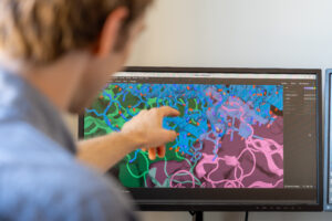
“The University of Washington is well-known for its expertise in nanoscale materials, processing, physics and biology — as well as its cutting-edge nanofabrication, characterization and testing facilities,” Karl Böhringer, the institute’s director, said in UW’s account of Monday’s opening reception. “NanoES will build on these strengths, bringing together people, tools and opportunities to develop nanoscale devices and systems.”
UW’s other nano initiatives include its Molecular Engineering Materials Center, which recently received a $15.6 million federal grant; and the Washington Nanofabrication Facility, which recently completed a three-year, $37 million upgrade.
Böhringer is coming over to NanoES from the nanofabrication facility, and other UW researchers will be relocating in the institute as well. One such researcher is Eric Klavins, a UW professor of electrical engineering who moved part of his synthetic biology team to the building.
The shift will put those team members in closer proximity to colleagues in the Molecular Engineering and Sciences Building, which is adjacent to NanoES. “We are extremely excited about the interdisciplinary and collaborative potential of the new space,” Klavins said.
UW listed three research priorities for NanoES, which is part of the university’s College of Engineering:
- Augmented humanity, which includes technology to both aid and replace human capability in a way that joins user and machine as one – and foresees portable, wearable, implantable and networked technology for applications such as personalized medical care, among others.
- Integrated photonics, which ranges from single-photon sensors for health care diagnostic tests to large-scale, integrated networks of photonic devices.
- Scalable nanomanufacturing, which aims to develop low-cost, high-volume manufacturing processes for applications ranging from the 3-D printing of cell and tissue scaffolds to ultrathin solar cells.
NanoES already has produced its first spin-out company, Tunoptix, which was co-founded by Böhringer and recently received startup funding from IP Group, a British venture capital firm.
“We are eager to work with our partners at the IP Group to bring our technology to the market, and we appreciate their vision and investment in the NanoES Integrated Photonics Initiative,” said Tunoptix entrepreneurial lead Mike Robinson. “NanoES was the ideal environment in which to start our company.”